The Backside Revolution: Optimizing Power Integrity for Next-Gen Silicons
As chip fabrication moves toward sub-2nm nodes, the industry is shifting focus to Backside Power Networks (BSPDN) and Nano-TSVs. Optimizing these connections is critical for maintaining power integrity and reducing resistance in the high-density processors required for AI.
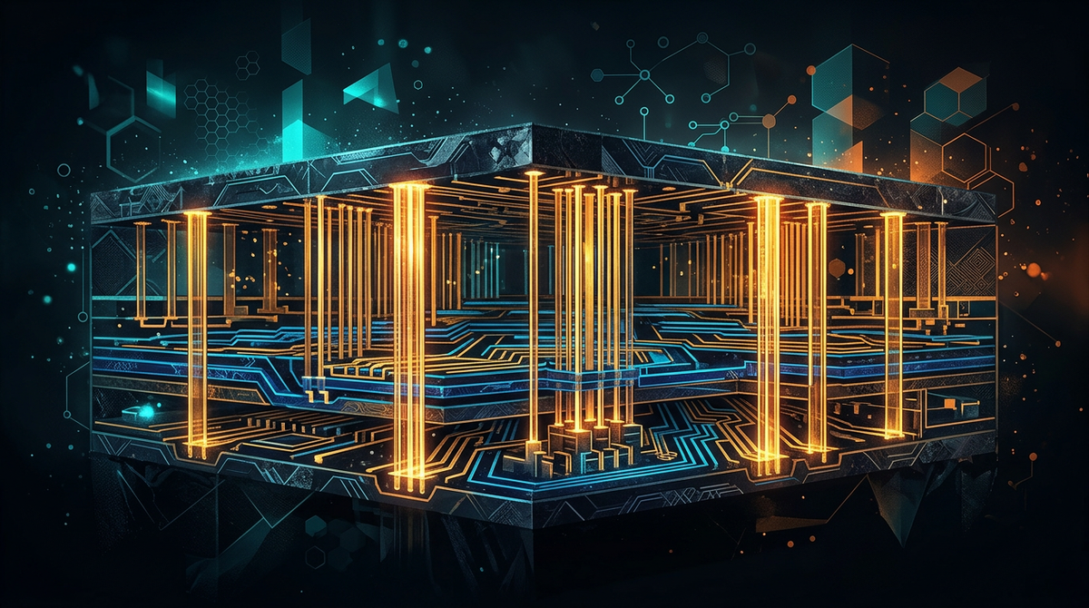
The semiconductor industry is hitting a wall with traditional front-side power delivery. As billions of transistors are packed into smaller footprints, the intricate web of wires required to deliver power and signals becomes a congested mess of resistance and heat. The solution appearing at the leading edge is Backside Power Delivery (BSPDN), a structural reconfiguration that moves the power distribution network to the underside of the wafer.
Recent research highlights the critical role of Nano-Through-Silicon Vias (nTSVs) in this new architecture. These tiny vertical connections link the backside power rails to the transistors on the front. However, at the nanometer scale, even the shape of these connections—such as rounded corners or misalignment during the bonding process—can significantly spike resistance and lower the efficiency of the chip. Virtual modeling is now being used to optimize the connection between nTSVs and Buried Power Rails (BPR), ensuring that power delivery remains stable even under the extreme workloads of AI training.
This shift is more than just a layout change; it is a fundamental redesign of how chips are manufactured. By separating the signal and power paths, engineers can reduce "voltage droop" and allow for higher clock speeds. For the Physical AI and robotics industries, which rely on high-performance-per-watt metrics, these semiconductor breakthroughs are the "hidden" drivers of capability. As fine-pitch hybrid bonding and BSPDN move into high-volume manufacturing, they will provide the thermal and electrical overhead necessary for the next leap in edge computing.
Source: Semiconductor Engineering