Vertical Challenges: The Struggle for Power Integrity in 3D-IC AI Chips
As AI models grow more complex, the hardware supporting them is evolving toward 3D integrated circuits (3D-ICs). Managing power integrity in these stacked architectures is now the primary challenge for semiconductor designers.
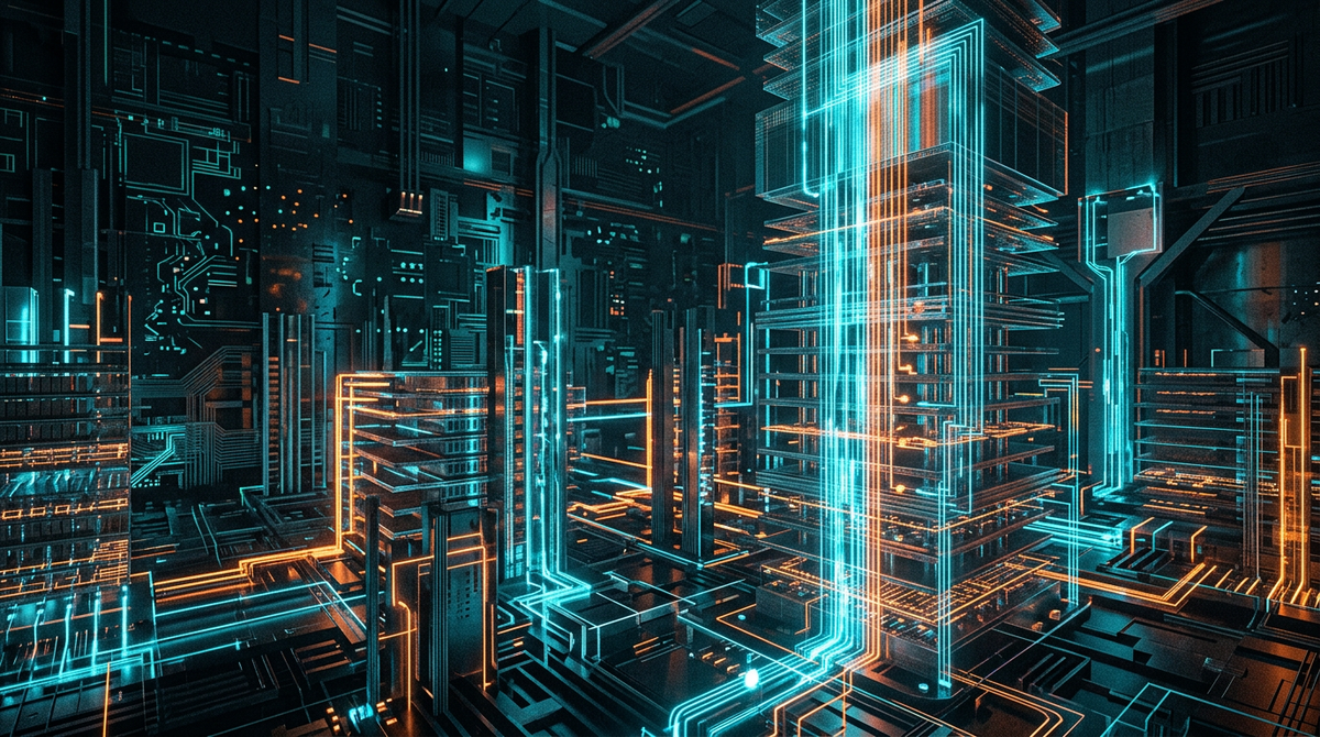
The insatiable demand for AI compute power has pushed traditional 2D chip design to its physical limits. To continue the trajectory of Moore’s Law, the semiconductor industry is pivoting toward 3D Integrated Circuits (3D-ICs), where layers of silicon are stacked vertically. While this vastly increases transistor density and reduces latency, it introduces a nightmare for power integrity.
In a 3D-IC, delivering consistent voltage to the middle of a silicon stack is incredibly difficult. Power integrity—ensuring that every part of the chip receives the exact electricity it needs without noise or drops—is now the dominant constraint in chip design. Designers must account for thermal hotspots where heat from one layer can degrade the performance of the layer above it, potentially leading to errors in AI inference.
The solution lies in new EDA (Electronic Design Automation) tools that can simulate the electromagnetic and thermal behavior of the entire stack simultaneously. This holistic approach to "Power Integrity" is no longer an afterthought; it is the blueprint. As we build the gigascale AI factories of the future, the success of these 3D architectures will determine whether we can continue to scale AI capabilities without melting the hardware.
Source: Semiconductor Engineering