The Kilowatt Challenge: Validating the Next Generation of AI Silicon
The rise of AI accelerators with over 1kW of power consumption is forcing a total redesign of semiconductor validation strategies. Engineers are now grappling with extreme thermal management and workload-specific testing to ensure reliability in the next generation of silicon.

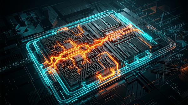
The race for AI supremacy has led to the development of Semiconductors that push the absolute limits of physics and power delivery. We are now entering the era of the "Kilowatt Chip," where a single AI accelerator can consume over 1,000 watts of power. This massive power draw is forcing a fundamental rethink of validation and testing strategies. At this level of density, traditional cooling methods fail, and the thermal expansion of the silicon itself can lead to structural failures or "silent data errors."
Validating these chips is no longer just about logic gates; it’s about thermal management. Engineers must now test chips across a wide range of "workload profiles," as the heat generated by a Large Language Model (LLM) training session differs significantly from simpler inference tasks. If the power delivery network (PDN) fluctuates by even a fraction of a percent at 1kW, it can cause transient errors that are notoriously difficult to debug in the field. This has led to the rise of "fleet monitoring," where the chip’s health is tracked in real-time throughout its lifecycle in the data center.
Furthermore, as we approach sub-2nm processes, the physical dimensions of the transistors are so small that quantum tunneling and other microscopic phenomena become major hurdles. The semiconductor industry is responding by merging discrete manufacturing steps and adopting new materials like SiCr for better process control. The future of AI hinges on the ability to reliably produce these high-power monsters, making validation the new frontline in the global chip war.
Source: Semiconductor Engineering