Angstrom-Scale Innovation: Backside Power and Chiplet Yields
As semiconductor dimensions reach the angstrom level, researchers are exploring backside power delivery and defect-aware chiplet matching to overcome physics-based limitations and optimize yield.
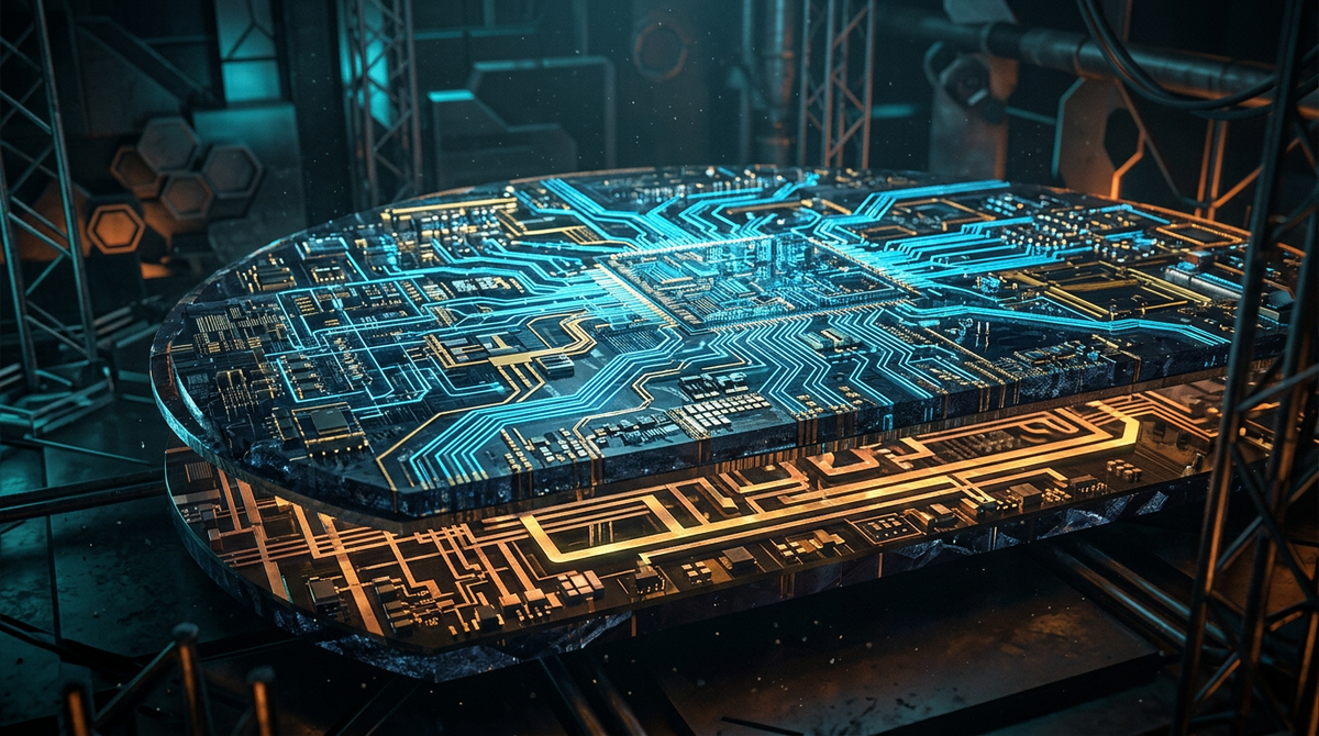
The Angstrom Era: Engineering Around Physics
The semiconductor industry is entering a realm where traditional scaling laws are being pushed to their absolute physical limits. As we move toward angstrom-level dimensions, the "Physics vs. Data" debate has become central to chip design. Researchers are increasingly finding that at these scales, quantum effects and thermal noise cannot be managed by data-driven models alone; they require a fundamental rethink of chip architecture.
One of the most promising breakthroughs discussed in recent technical papers is Backside Power Delivery (BSPDN). By moving the power distribution network to the back of the silicon wafer, engineers can reduce "voltage droop" and free up space on the front side for more signal routing. Recent research from KAIST even proposes a "Backside Clock Mesh," which significantly reduces clock skew and power consumption, addressing two of the biggest hurdles in modern high-performance computing.
Furthermore, the industry is embracing heterogeneous integration through chiplets. However, this creates a yield problem: if one chiplet in a multi-chip module is defective, the whole package is ruined. New "Defect-Aware Chiplet Matching" techniques are being developed to optimize these yields. By using AI to match chiplets with compatible performance profiles and minor defects, manufacturers can salvage components that would otherwise be discarded, ensuring that the next generation of AI hardware remains economically viable despite its staggering complexity.
Source: Semiconductor Engineering