Powering the AI Surge: Redefining Silicon Margins and Delivery Networks
AI accelerators are forcing a radical redesign of power delivery networks and silicon margin characterization to maintain yield in the age of high-performance computing.
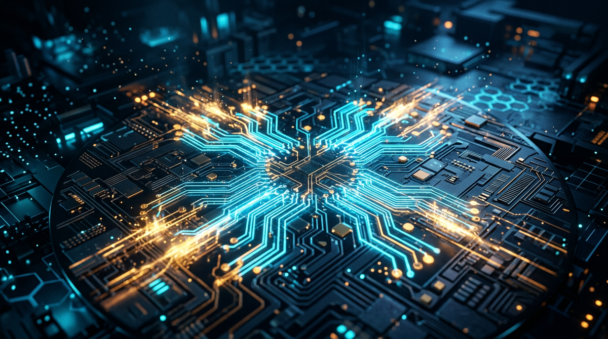
The explosive demand for AI accelerators is pushing semiconductor engineering to its physical limits. As chips grow larger and more power-hungry, the industry is witnessing a total overhaul of Power Delivery Networks (PDNs). Moving voltage regulators closer to the processor is no longer an option but a necessity to reduce power loss, yet this introduces significant challenges in advanced packaging and thermal management.
To maintain yield in these complex designs, engineers are moving "Beyond Pass/Fail." Characterizing silicon margin with PVTW (Process, Voltage, Temperature, and Workload) allows designers to understand exactly how far a device is from its functional boundary. This data-driven approach is essential for high-performance AI silicon, where even minor variations can lead to catastrophic failure in a data center environment.
Furthermore, the use of "Virtual Twins" and machine learning is now being applied to DRAM yield optimization. By modeling process variations and detecting multiple failure modes before a single wafer is etched, manufacturers can scale innovation while maintaining the quality required for the next generation of AI hardware. The recovery of silicon wafer demand is being driven by this cycle of high-performance infrastructure, marking a unique period of growth for the semiconductor stack.
Source: Semiconductor Engineering