2nm and Beyond: Why Multi-Die Assemblies Are the Future of AI Silicon
As we approach the 2nm node and beyond, the semiconductor industry is shifting toward multi-die assemblies. These modular architectures are essential for meeting the massive compute and efficiency demands of the AI era.
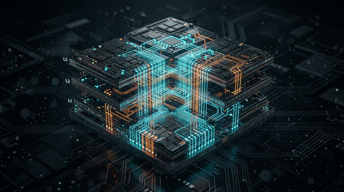
The era of the monolithic chip is drawing to a close at the leading edge. As semiconductor manufacturing pushes toward 2nm and below, the physical and economic limits of single-die processors are becoming insurmountable. The solution, now dominating the industry, is multi-die assemblies—often referred to as "chiplets."
By breaking a large processor into smaller, modular components, manufacturers can mix and match different process nodes and specialized functions. This modularity is critical for the "AI Factories" being built today, where the balance between performance and power consumption is paramount. For example, NVIDIA’s Vera Rubin architecture leverages advanced interconnects like NVLink to fuse multiple dies into a single high-performance unit, achieving up to 30x more work per watt for agentic AI workloads.
This shift requires a revolution in packaging and monitoring. Multi-die assemblies introduce new challenges in thermal management and signal integrity. However, the benefits—higher yields, faster time-to-market, and the ability to scale compute to unprecedented levels—make this the only viable path forward for the semiconductors that power the infrastructure of intelligence.
Source: Semiconductor Engineering